<small id="v9s5k"></small><label id="v9s5k"><menuitem id="v9s5k"><font id="v9s5k"></font></menuitem></label>

      Stock Code:002815
      中文
      Jiangsu IC Substrate plant

      Founded in 2004 in Kunshan,  Jiangsu ProVision Electronics Co., Ltd. ( ProVision) is a holding subsidiary of Suntak Technology Co., Ltd. It is mainly specialized in producing integrated circuit substrate boards. The company is engaged in becoming a hidden champion of the segmented industry, and taking a leading role in the technology and manufacture of MEMS package substrates. The products are mainly applied in smart phones, automotives, PC, wearable devices, smart home, medical, PV, servers, inverters and other fields. 

      • 32,000㎡

      • 500+

      • Mobile Phone, Wearable, Tablet

      • 15,000㎡

      • SiPSubstrate

        Craft show

        Layers 2 -8L
        Strip Size 189.0*68.0,70.0*240.0,75.0*240.0, 76.3*240.0, 95.0*240.5etc.
        Unit Size 5.4*6.8,8.1*8.1 / 15*16/ 19*19 etc.
        Material MGC 832NXA / 832NS / 972 Series Hitachi 705G/ 770G Series AUS308 / AUS 320 / SR1
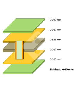
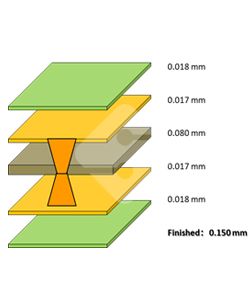
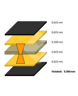
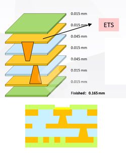
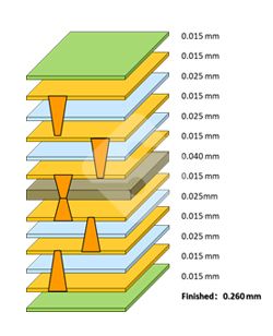
        Finished Thickness 0.120~0.500 mm
        Min. Trace Width/Space 0.025mm / 0.025 mm
        Product Feature Impedance,Selected OSP, SM Coining
        Applications Wearables,Wireless etc.
      • FingerPrintSubstrate

        Craft show

        Layers 2-4L
        Strip Size 75.0*240.0,76.3*240.0etc.
        Unit Size 1.5*4.0 etc
        Material Doosan 7409HGB(LE)/(GQ) Series AUS308
        Finished Thickness 0.500~0.800 mm
        Min. Trace Width/Space 0.040mm / 0.040 mm
        Product Feature SM Coining
        Applications Phone,Wearables,PCetc.
      • Pressure sensor substrate

        Craft show

        Layers 2 ~4 L
        Strip Size 66.0*142.0,50.8*188.95,50.8*152.4, 74.0*240.0,75.0*240.0,76.3*240.0etc.
        Unit Size 2*2/ 3*3 etc.
        Material MGC 832NXA / 832NS Series SYL SI13U / SI10US Series AUS308
        Finished Thickness 0.120~0.500 mm
        Min. Trace Width/Space 0.040mm / 0.040 mm
        Product Feature SM Coining
        Applications Phone,Wearables,PC,Automobileetc.
      • Light Sensor Substrate

        Craft show

        Layers 2 ~4 L
        Strip Size 50.8*188.95,187.5*50.0etc.
        Unit Size 1.5*4.2 etc.
        Material MGC 832NXA / 832NS Series NANYA NPG-180BK / INBK Series AUSMEH / EG23
        Finished Thickness 0.200~0.500 mm
        Min. Trace Width/Space 0.040mm / 0.040 mm
        Product Feature 油墨整平
        Applications Phoneetc.
      • Filter Substrate

        Craft show

        Layers 2~4 L
        Strip Size 93.81*93.81,189.0*68.0,75.0*240.0, 100.0*103.0,76.3*240.0etc.
        Unit Size 1814 / 1612 / 1411 / 1109 etc.
        Material MGC 832NS Series Hitachi 705GSeries AUS308 / AUS 320
        Finished Thickness 0.120~0.300 mm
        Min. Trace Width/Space 0.025mm / 0.025 mm
        Product Feature Coreless Structure,ETS Structure
        Applications Phone,Wearablesetc.
    1. Goertek Quality Award

    2. MEMSensing Quality Award

    3. Mitsui Copper Foil

    4. China's heavy quality, Shou credibility

    5. Technical Research Center

    6. Small giant enterprise

    7. Credit management model enterprise

    8. Circuit industry association

    9. Top 10 growth companies

    10. Ten best Harmonious labor

    11. Become a world-leading manufacturer of Circuit board

      Follow us

      一级a一级a爰片免费免两_亚洲成av人精品自偷拍_亚洲ⅴa中文字幕无码毛片_亚洲黄无码一区二区三区
      <small id="v9s5k"></small><label id="v9s5k"><menuitem id="v9s5k"><font id="v9s5k"></font></menuitem></label>

          久久精品中文字幕欲求不满 | 日韩不卡一区二区三区 | 一区二区免费不卡在线 | 精品国产偷窥丝袜在线拍国语 | 日韩一级在线视频一区 | 亚洲五月丁香中文字幕 |